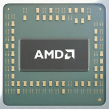
AMD Mobile Athlon 64 3700+ vs Intel Core 2 Duo U7600
Physical Specifications
| Socket | AMD Socket 754 | Intel Socket P |
|---|---|---|
| Process size | 130 nm | 65 nm |
| Transistors | 106 million | 293 million |
| Die size | 193 mm² | 111 mm² |
| Package | µPGA | FC-PGA |
| Foundry | — | Intel |
Performance
| Frequency | 2.4 GHz | 1200 MHz |
|---|---|---|
| Turbo clock | — | — |
| Base clock | 2400 MHz | 133 MHz |
| Multiplier | 12.0x | 9.0x |
| Multiplier unlocked | No | No |
| Voltage | 1.5 V | 0.975 V |
| TDP | 82 W | 10 W |
Architecture Details
| Vertical Segment | Mobile | Mobile |
|---|---|---|
| Production status | End-of-life | End-of-life |
| Release date | Aug 1st, 2005 | Apr 27th, 2007 |
| Codename | Clawhammer | Merom |
| Generation | Mobile Athlon 64 | Core 2 Duo |
| Part | AMA3700BEX5APAMA3700BEX5AR | SLV3W |
| Memory support | DDR1 Single-channel | unknown |
| ECC memory | No | No |
Cores
| Total Cores | 1 | 2 |
|---|---|---|
| Total Threads | 1 | 2 |
| SMP # CPUs | 1 | 1 |
| Integrated graphics | — | — |
Cache
| Cache L1 | 128K | 64K |
|---|---|---|
| Cache L2 | 1MB | 2MB |
Notes
| Notes | Stepping: AMA3700BEX5AP C0/AMA3700BEX5AR CG | — |
|---|
Features & Technologies
| 3DNow! | Yes | — |
|---|---|---|
| AMD64 | Yes | — |
| EIST | — | Yes |
| Intel 64 | — | Yes |
| MMX | Yes | Yes |
| SSE | Yes | Yes |
| SSE2 | Yes | Yes |
| SSE3 | — | Yes |
| SSSE3 | — | Yes |
| VT-x | — | Yes |
| XD bit | — | Yes |

