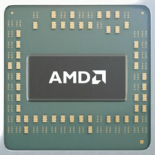
AMD Athlon 64 X2 4200+ vs Intel Core i7-4600M
Physical Specifications
| Socket | AMD Socket AM2 | Intel Socket G3 |
|---|---|---|
| Process size | 90 nm | 22 nm |
| Transistors | 154 million | 1,300 million |
| Die size | 220 mm² | 118 mm² |
| Package | µPGA | FC-PGA946 |
| Foundry | — | Intel |
| tCaseMax | — | 100°C |
Performance
| Frequency | 2.2 GHz | 2.9 GHz |
|---|---|---|
| Turbo clock | — | up to 3.6 GHz |
| Base clock | 200 MHz | 100 MHz |
| Multiplier | 11.0x | 29.0x |
| Multiplier unlocked | No | No |
| Voltage | 1.35 V | — |
| TDP | 89 W | 37 W |
Architecture Details
| Vertical Segment | Desktop | Mobile |
|---|---|---|
| Production status | End-of-life | Active |
| Release date | May 23rd, 2006 | Sep 1st, 2013 |
| Codename | Windsor | Haswell |
| Generation | Athlon 64 X2 | Core i7 |
| Part | ADA4200IAA5CU | SR1H7 |
| Memory support | unknown Dual-channel | DDR3 |
| ECC memory | No | No |
| PCI Express | Gen 2 | — |
Cores
| Total Cores | 2 | 2 |
|---|---|---|
| Total Threads | 2 | 4 |
| SMP # CPUs | 1 | 1 |
| Integrated graphics | — | Intel HD 4600 |
Cache
| Cache L1 | 256K | 64K (per core) |
|---|---|---|
| Cache L2 | 512K | 256K (per core) |
| Cache L3 | — | 4MB (shared) |
Features & Technologies
| 3DNow! | Yes | — |
|---|---|---|
| AES-NI | — | Yes |
| AMD-V | Yes | — |
| AMD64 | Yes | — |
| AVX | — | Yes |
| AVX2 | — | Yes |
| CLMUL | — | Yes |
| EIST | — | Yes |
| FMA3 | — | Yes |
| HTT | — | Yes |
| Intel 64 | — | Yes |
| MMX | Yes | Yes |
| SSE | Yes | Yes |
| SSE2 | Yes | Yes |
| SSE3 | Yes | Yes |
| SSE4.2 | — | Yes |
| SSSE3 | — | Yes |
| TSX | — | Yes |
| TXT | — | Yes |
| VT-x | — | Yes |
| XD bit | — | Yes |

