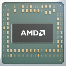
AMD A10-9700E vs AMD Phenom X4 9600
Physical Specifications
| Socket | AMD Socket AM4 | AMD Socket AM2+ |
|---|---|---|
| Process size | 28 nm | 65 nm |
| Transistors | 1,178 million | 450 million |
| Die size | 246 mm² | 285 mm² |
| Package | µPGA | µPGA |
| tCaseMax | 74°C | — |
Performance
| Frequency | 3 GHz | 2.3 GHz |
|---|---|---|
| Turbo clock | up to 3.5 GHz | — |
| Base clock | 100 MHz | 200 MHz |
| Multiplier | 30.0x | 11.5x |
| Multiplier unlocked | Yes | No |
| Voltage | 1.475 V | 1.25 V |
| TDP | 35 W | 95 W |
Architecture Details
| Vertical Segment | Desktop | Desktop |
|---|---|---|
| Production status | Active | End-of-life |
| Release date | Jul 27th, 2017 | Nov 19th, 2007 |
| Codename | Bristol Ridge | Agena |
| Generation | A10 | Phenom X4 |
| Part | AD9700AHM44AB | HD9600WCJ4BGD |
| Memory support | DDR4 Dual-channel | unknown Dual-channel |
| ECC memory | No | No |
| PCI Express | — | Gen 2 |
Cores
| Total Cores | 4 | 4 |
|---|---|---|
| Total Threads | 4 | 4 |
| SMP # CPUs | 1 | 1 |
| Integrated graphics | Radeon R7 | — |
Cache
| Cache L1 | 128K (per core) | 128K (per core) |
|---|---|---|
| Cache L2 | 1MB (per core) | 512K (per core) |
| Cache L3 | — | 2MB (shared) |
Notes
| Notes | This processor comes with an unlocked base clock multiplier, allowing users to set the multiplier value higher than shipped value, to facilitate better overclocking. | Processor with the older B2 revision and TLB Bug. |
|---|
Features & Technologies
| 3DNow! | Yes | Yes |
|---|---|---|
| AES | Yes | — |
| AMD-V | Yes | Yes |
| AMD64 | Yes | Yes |
| AVX | Yes | — |
| AVX2 | Yes | — |
| BMI1 | Yes | — |
| BMI2 | Yes | — |
| CnQ | — | Yes |
| EVP | Yes | — |
| F16C | Yes | — |
| FMA3 | Yes | — |
| FMA4 | Yes | — |
| HT3.0 | — | Yes |
| MMX | Yes | Yes |
| NX bit | — | Yes |
| SSE | Yes | Yes |
| SSE2 | Yes | Yes |
| SSE3 | Yes | Yes |
| SSE4 | Yes | — |
| SSE4.1 | Yes | — |
| SSE4.2 | Yes | — |
| SSE4A | Yes | Yes |
| TBM | Yes | — |
| Turbo Core | Yes | — |
| XOP | Yes | — |

