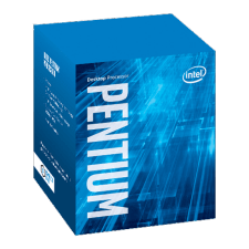
Intel Pentium P6200 vs Intel Pentium P6300
Physical Specifications
| Socket | Intel Socket G1 | Intel Socket G1 |
|---|---|---|
| Foundry | Intel | Intel |
| Process size | 32 nm | 32 nm |
| Transistors | 384 million | 384 million |
| Die size | 81 mm² | 81 mm² |
| Package | rPGA | rPGA |
Performance
| Frequency | 2.133 GHz | 2.266 GHz |
|---|---|---|
| Turbo clock | — | — |
| Base clock | 133 MHz | 133 MHz |
| Multiplier | 16.0x | 17.0x |
| Multiplier unlocked | No | No |
| TDP | 35 W | 35 W |
Architecture Details
| Vertical Segment | Mobile | Mobile |
|---|---|---|
| Production status | End-of-life | End-of-life |
| Release date | Sep 26th, 2010 | Jan 9th, 2011 |
| Codename | Arrandale | Arrandale |
| Generation | Pentium | Pentium |
| Part | SLBUA | SLBU8 |
| Memory support | DDR3 | DDR3 |
| ECC memory | No | No |
| PCI Express | Gen 2 | Gen 2 |
Cores
| Total Cores | 2 | 2 |
|---|---|---|
| Total Threads | 2 | 2 |
| SMP # CPUs | 1 | 1 |
| Integrated graphics | — | — |
Cache
| Cache L1 | 64K (per core) | 64K (per core) |
|---|---|---|
| Cache L2 | 256K (per core) | 256K (per core) |
| Cache L3 | 3MB (shared) | 3MB (shared) |
Notes
| Notes | 177M GPU Transistors | 177M GPU Transistors |
|---|
Features & Technologies
| EIST | Yes | Yes |
|---|---|---|
| Intel 64 | Yes | Yes |
| MMX | Yes | Yes |
| SSE | Yes | Yes |
| SSE2 | Yes | Yes |
| SSE3 | Yes | Yes |
| SSSE3 | Yes | Yes |
| Smart Cache | Yes | Yes |
| XD bit | Yes | Yes |
